What is the Difference Between Positive and Negative PCB Circuit Board?
2020-06-13
As a Finishing PCB Technologies Supplier, share with you. Negative film of PCB circuit board: It is generally the tenting process we talk about.The chemical solution used is an acid etching negative film because after the negative film is produced, the desired circuit or copper surface is transparent, and the unnecessary part is black. After exposure through the circuit process, the transparent part is chemically hardened due to the exposure of the dry film resist to light.The subsequent development process will wash away the unhardened dry film, so only the dry film washout is bitten during the etching process part of the copper foil (the black part of the negative), and the dry film is not washed out and belongs to the circuit we want (the transparent part of the negative)
Positive film of PCB circuit board: Generally it is the pattern process we talk about. The yao liquid used is alkaline etching positive film. If viewed from the negative film, the desired circuit or copper surface is black, and the part is transparent. Similarly, after exposure through the circuit process, the transparent part is chemically hardened due to the dry film resist being exposed to light.The next development process will wash away the unhardened dry film, followed by the tin-lead plating process to remove tin-lead Plating on the copper surface washed away by the dry film of the previous process (development), and then the film removal action (removing the dry film hardened by light), and in the next process etching, the alkaline tin water is used to bite off the tin. Lead-protected copper foil (transparent part of the negative), the rest is the circuit we want (black part of the negative)
The positive film and negative film are actually selected according to the process of each circuit board factory. The positive film: the process is (double-sided circuit board) blanking-drilling-PTH (one-time plating is also called thickening copper)-circuit-two copper (graphic plating ) Then take the SES line (removing film-etching-removing tin) negative film: the process is (double-sided) blanking-drilling-PTH (one-time plating is also called thickening copper)-circuit (without two copper pattern plating) and then go DES line (etching-removing film)
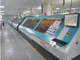
Our company also has Flexible PCBs for sale, please contact us.