Do you know the Clock Circuit Designed in the PCB?
2020-09-08
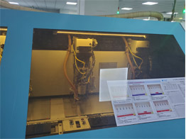
As a PCB Fabrication Company, share with you. In a circuit system, the clock is an essential part. Like the human heart, if the clock of the circuit system is wrong, the system will be disordered. Therefore, a good clock circuit is very necessary to design in the PCB. Our commonly used clock circuits are: crystals, crystal oscillators, and distributors. The clock used by some ICs may be generated by the main chip, but when traced to the source, it is generated by one of the above three.
Crystals:
1. The pin should be as close as possible to the chip to prevent interference from other signals. Of course, prevent it from interfering with other lines, because it is the signal source.
2. Try to choose iron case crystal oscillator, which has stronger anti-interference ability.
3. All layers below the crystal oscillator cannot be routed, and GND copper should be laid.
4. Do not have too close digital signal lines near the crystal oscillator.
5. The return ground of the load capacitor must be short.
6. GND surround the crystal oscillator. Open the window to leak GND copper in some places, and solder the crystal housing to the place where the window leaks GND copper.
7. Pass the capacitor first and then the crystal oscillator during layout
Commonly used crystal packages in PCB are: 2-pin plug-in package, SMD package, 4-pin SMD package
Although crystals have different specifications, their basic circuit design is the same. Therefore, PCB layout and wiring regulations
It is also universal.
In the crystal circuit layout, two capacitors are placed close to the crystal:
When wiring, the pair of lines of the crystal should be in the form of differential-like, and the lines should be as short as possible, thickened and grounded.
In combination with the above, the layout should pay attention to:
1. It is placed on the same layer as the IC, so that fewer holes can be punched;
2. The layout should be compact, the capacitor should be located between the crystal and the IC, and placed close to the crystal, so that the clock line to the IC should be as close as possible
short;
3. In the case of test points, try to avoid stubs or make stubs as short as possible;
4. Do not place amplifying power devices, such as power chips, MOS tubes, inductors and other devices with high heat generation nearby;
Wiring should pay attention to:
1. Layout on the same layer as the IC, wiring on the same layer, and punch as little as possible. If punching, you need to add return ground holes nearby;
2. Class differential wiring;
3. The trace should be thicker, usually 8~12mil; since the crystal clock waveform is a sine wave, so here is designed according to simulation
Idea processing;
4. The signal wire is covered with ground, and the ground wire or copper sheet must be shielded with ground holes;
5. The crystal circuit module area is equivalent to the analog area, try not to have other signals passing through;
Our company also hasFlexible PCBs on sale, please contact us.